-
 Get UpdatesGet notified on education trends, resources, and growth opportunities!
 -

-


 Click it and Unblock the Notifications
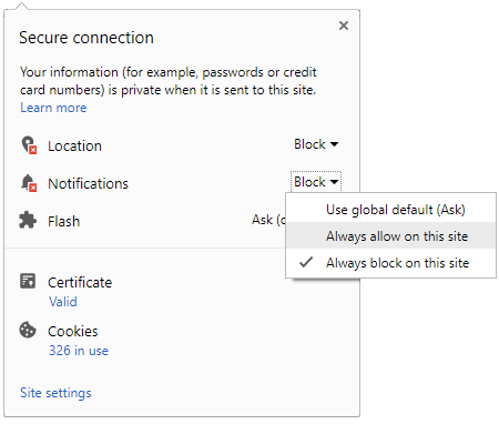
BITS Pilani Collaborates with Siemens to Launch Program in PCB Design
Birla Institute of Technology and Science (BITS) Pilani has partnered with Siemens EDA to launch a joint certification programme in PCB Design and Analysis, aimed at strengthening industry-relevant skills in electronics and semiconductor engineering. The initiative is part of BITS Pilani's Work Integrated Learning Programmes (WILP), designed to bridge the gap between academic learning and practical industry demands.

Details of the Collaboration
Under this collaboration, BITS Pilani WILP and Siemens EDA will offer a specialised certification that focuses on printed circuit board (PCB) design, simulation, and analysis. The programme is structured to help learners gain hands-on expertise in areas such as:
- Schematic and multilayer PCB design
- High-speed signal integrity and power integrity
- EMI/EMC analysis
- Practical use of Siemens EDA's Xpedition and HyperLynx platforms
These tools are widely used in industry for designing complex electronic systems and ensuring they meet performance and compliance standards, making the certification valuable for careers in semiconductor, automotive electronics and industrial automation.
Who Can Benefit
The programme is open to a broad audience, including:
- Students pursuing engineering and related degrees
- Working professionals seeking to upskill
- Industry engineers looking to enhance practical PCB design capabilities
By combining theoretical foundations with practical, real-world tools, the certification aims to create a pipeline of engineers ready to contribute to India's growing electronics and semiconductor ecosystem.
Industry Relevance
The electronics and semiconductor sectors are experiencing rapid growth in India, fuelled by initiatives such as Make in India, Semicon India Programme and increased global demand for locally designed and manufactured products.
PCB design and analysis are fundamental skills in electronics development, driving demand for engineers who can work effectively with advanced computer-aided design (CAD) tools and handle real-world design challenges.
Statements from Leadership
According to BITS Pilani WILP leadership, the collaboration underscores the importance of industry-academia partnerships for meaningful educational outcomes. By integrating industry tools and processes into academic offerings, students and professionals can develop skills that align directly with employer needs.
Siemens EDA representatives have similarly emphasized the programme's role in building future-ready engineers equipped with practical design and analysis capabilities used in modern electronics industries.
Why This Matters for Students
- Industry exposure: Training on actual tools used by electronics professionals.
- Skill enhancement: Focus on highly sought-after PCB design competencies.
- Career readiness: Equips learners for roles in semiconductors, hardware design and embedded systems.
As the Indian electronics ecosystem continues to expand, programmes like this collaboration between BITS Pilani and Siemens are expected to play a key role in preparing a workforce that is skilled, adaptable and ready for emerging technology challenges.
Conclusion
The BITS Pilani-Siemens PCB Design and Analysis programme represents a significant step in aligning education with industry requirements in engineering and technology. By focusing on practical certification, the collaboration aims to build a strong foundation for students and professionals seeking to advance careers in electronics, semiconductors and related fields.
More From Career India


- Block for 8 hours
- Block for 12 hours
- Block for 24 hours
- Don't block
- Male
- Female
- Others
- Under 18
- 18 to 25
- 26 to 35
- 36 to 45
- 45 to 55
- 55+