

 Click it and Unblock the Notifications
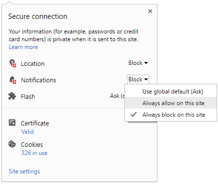

Anna University is conducting a short term course on physical sciences in the field of molecules, particularly Molecular Beam Epitaxy (MBE) technology.
What is Molecular Beam Epitaxy (MBE) technology?
Molecular Beam Epitaxy (MBE) technology was developed in response to the increasing attention paid by the semiconductor community to GaAs devices of increasing complexity and more to low dimensional structures. MBE is an epitaxial deposition technique which involves laying down layers of materials with atomic thicknesses on to substrates.
Importance of MBE
MBE has expanded in importance over the past thirty years from a pure research domain into commercial applications. MBE is important because it enables new device phenomena and facilitates the production of multiple layered structures with extremely fine dimensional and compositional control. The technique can be deployed wherever precise thin-film devices with enhanced and unique properties for computing, optics or photonics are required.
What does the course offer?
This course will include the research fundamentals technology and design of Molecular Beam Epitaxy, Impact made by MBE in research, an advanced deposition technique for semiconductor optoelectronic, photovoltaic and electronic devices and production epitaxial technology of MBE.
The main objective of this course is to train the participants to the fundamentals of technologically important semiconductors and functional materials and to enhance the capability of the participants to identify, control and manipulate device structures through better understanding of defects using DLTS.
")
Name of the course:
Low Dimensional Structures and Devices: From Research to Industry
Organiser:
Key points covered:
- Technology and design of Molecular Beam Epitaxy
- Manuscript Discussions
- Impact made by MBE in research
- Semiconductor optoelectronic, photovoltaic and electronic devices
- MBE as a production epitaxial technology
- Study of Defects
- Importance of DLTS and Analysis of Data
- Device Structure
Objectives:
i) Training the participants to the fundamentals of technologically important semiconductors and functional materials
ii) Providing the technical details on Molecular Beam Epitaxy to realise quantum structures.
iii) Enabling the participants to design, integrate complex multiple systems including growth of layered structures of specific
dimensions and characteristics
iv) Enhancing the capability of the participants to identify, control and manipulate device structures through better
understanding of defects using DLTS.
Eligibility:
- Executives, engineers and researchers from manufacturing, service and government organizations including R&D laboratories.
- Student students at all levels (BTech/MSc/MTech/PhD) or faculty from reputed academic institutions and technical institutions.
Fee:
The participation fees for taking the course is as follows:
- Participants from abroad: US $500
- Industry/ Research Organizations: Rs.3000
- Academic Institutions Staffs/faculty: Rs.2000
- Academic Institutions students: Rs.1000
The participants will have to take care of their travel, accommodation and food. For any queries
regarding registration or other practical information, please contact the Coordinator/Local co-ordinator
When:
January 6 th to 12 th 2017
Where:
Anna University
Number of seats:
Fifty
How to apply:
Contact the course co-ordinators through https://www.annauniv.edu/gian/contactus.html
Last date of admission:
NA
Foreign Faculty
Dr.Mohamed Henini, University of Nottingham, , United Kingdom
Host Faculty
Dr. J. Kumar, Crystal Growth Centre,Anna University
Website: https://www.annauniv.edu/pdf/gianbrochure-LowDimensionalStructures - Copy.pdf


Just In
-

-

-

-


Don't Miss
-
 Razakar Review: Makrand Deshpande Film Makes Bold Attempt To Touch Sensitive Topic Of Hyderabad Genocide
 -
 Toyota Fortuner Leader Edition – Top Things You Need To Know
 -
 'I Spend Rs 85 lakh in my holidays': Virender Sehwag tells Adam Gilchrist how he refused BBL offer
 -
 RBI's Order To Kotak Mahindra Bank: No New Customers, No New Credit Cards
 -
 HMD Branded First Set of Android Smartphones Are Here!
 -
 Vodafone Idea FPO: Shares To Debut Tomorrow; GMP Hints Premium Listing; Shares Slump 9%
 -
 Mumbai Opens BMC Headquarters For Exclusive Heritage Tour
 -
 Summer Style: 6 Must-Try Colors To Stay Fashionably Cool Like B-Town Divas!


